Sample Project: Wireless Environmental Sensor Node
Battery-powered BLE sensor node measuring temperature, humidity and ambient light for building-monitoring applications, designed for multi-year operation from a single CR2477 coin cell. (Fictional example content.)
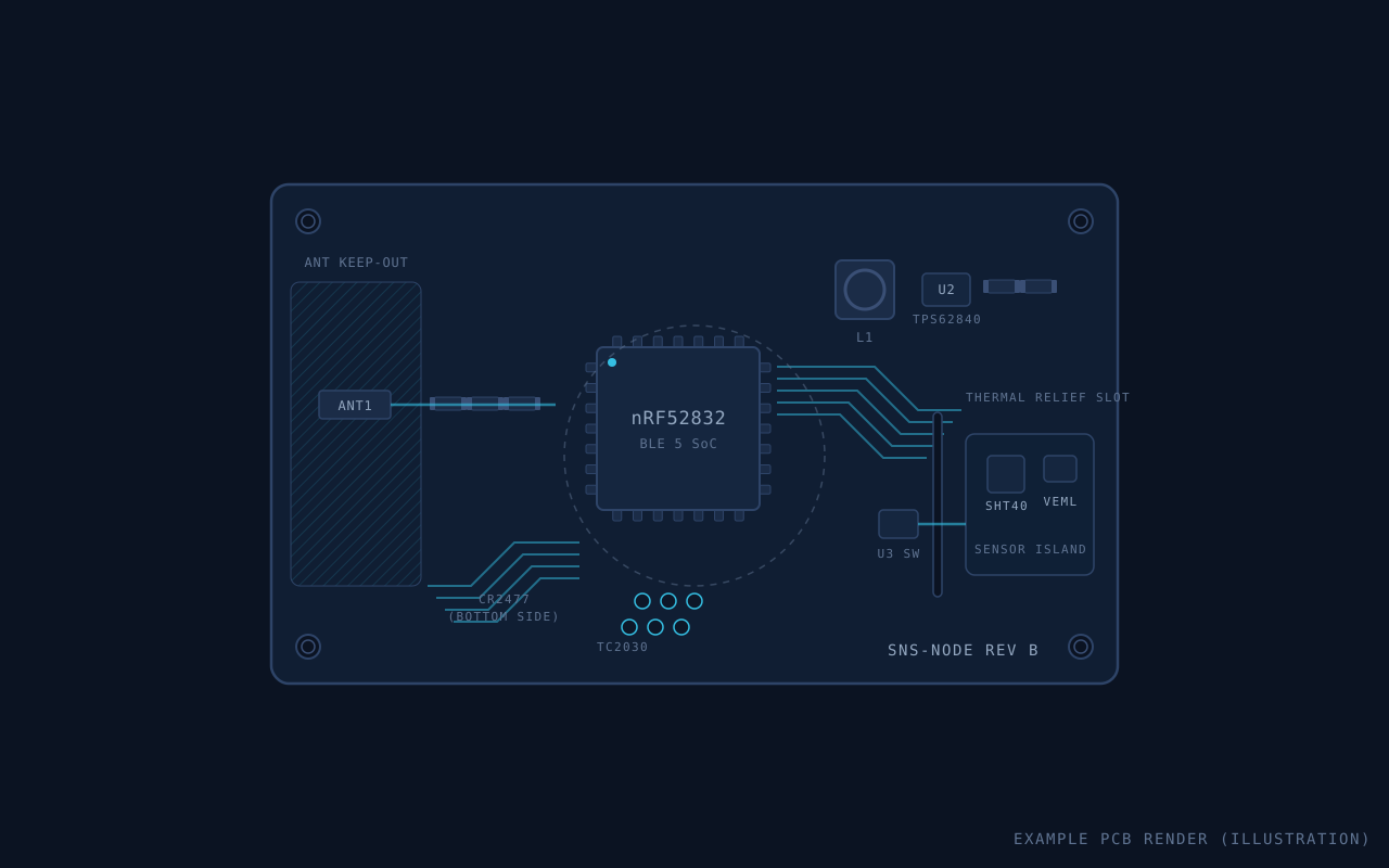
Product requirements
- Measure temperature (±0.2 °C), relative humidity (±2 %RH) and ambient light once per minute.
- Report over BLE advertising to existing gateways; no pairing or app required.
- Three-year battery life from a single CR2477 coin cell.
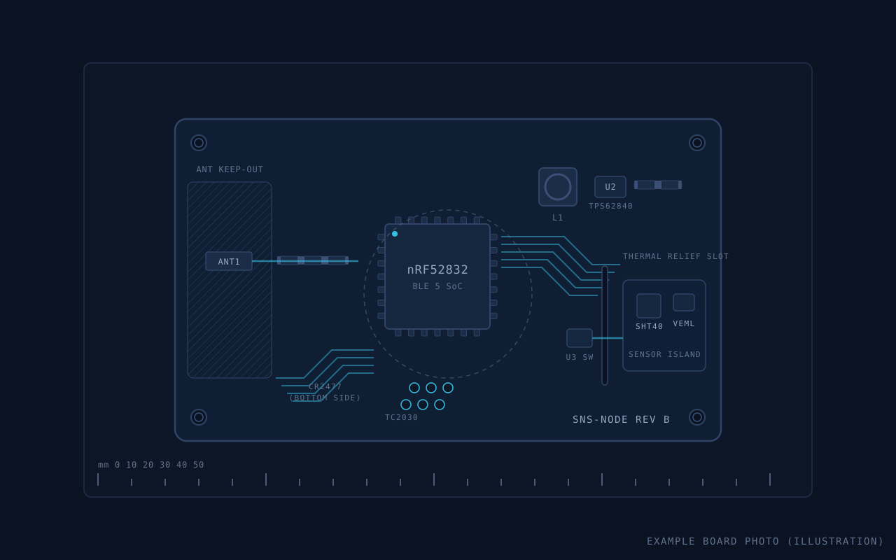
- Enclosure limited the board to 38 × 30 mm with a fixed mounting-hole pattern.
- Target BOM cost under a defined ceiling at 1k-unit volume; parts chosen for multi-source availability.
System architecture
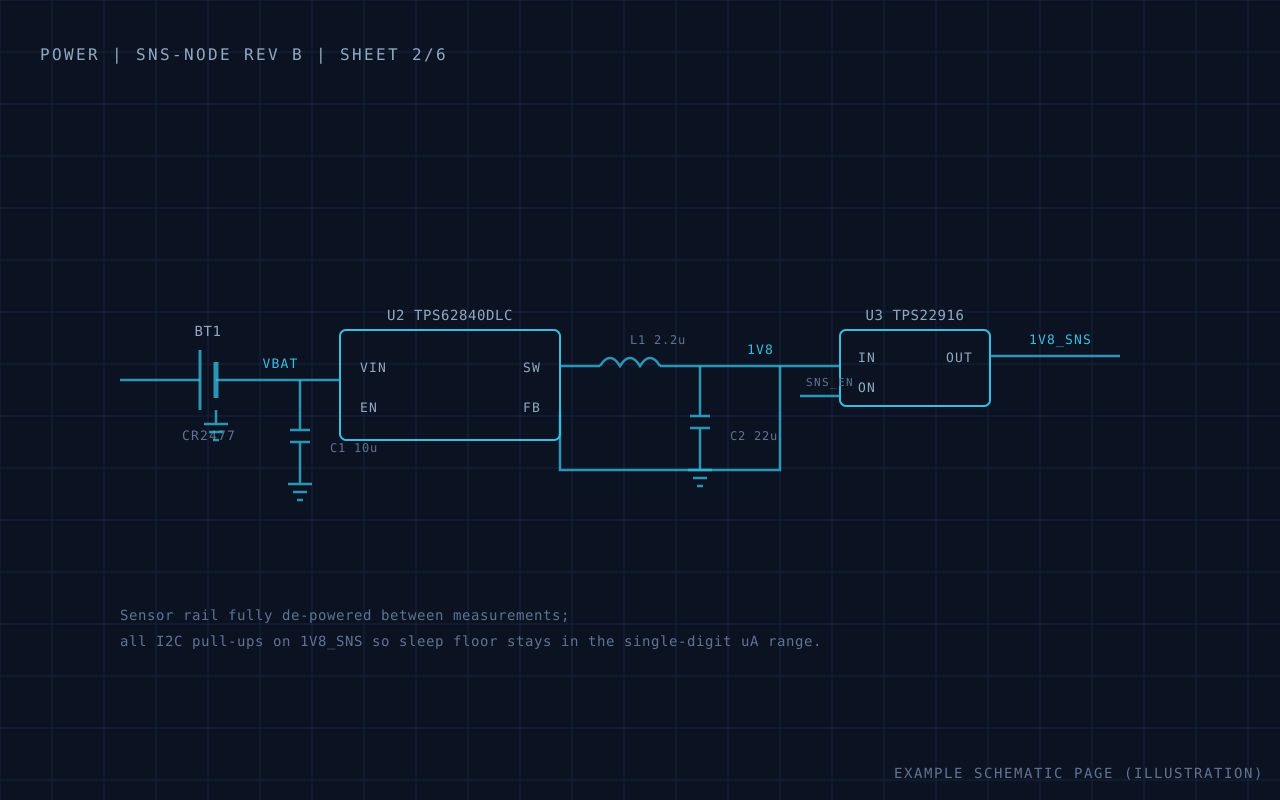
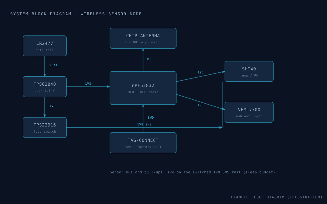
A single nRF52832 handles both application and radio. The sensors (SHT40 for temperature/humidity, VEML7700 for light) sit on a dedicated I²C bus behind a load switch so the whole sensor cluster can be fully de-powered between measurements. A TPS62840 buck converter steps the cell voltage down to 1.8 V for the digital domain; the radio runs in its DC/DC mode to cut TX current. Firmware wakes on an RTC tick, powers the sensors, samples, encodes the readings into a manufacturer-specific BLE advertisement and returns to system-off-like sleep.
Hardware design
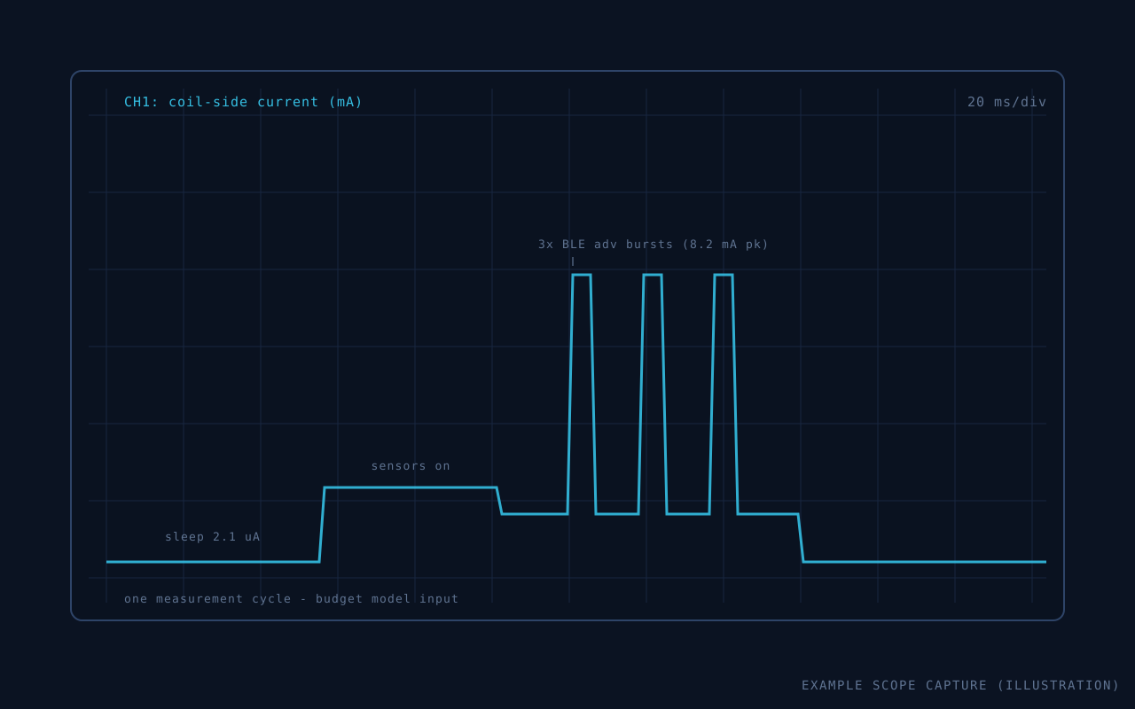
- Coin-cell power path with bulk storage capacitance sized for the 8 mA radio TX pulses, keeping cell voltage sag within the datasheet pulse-load limits.
- Load-switched sensor domain so sensor sleep current does not count against the battery budget.
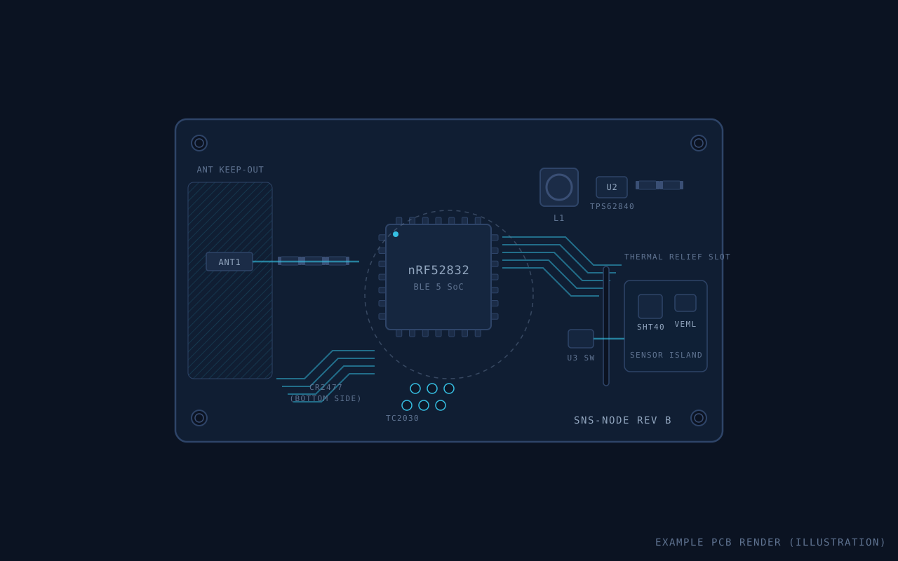
- SHT40 placed on a slot-isolated board region to decouple it from MCU self-heating.
- 2.4 GHz chip antenna with a ground keep-out and a π matching network placed for post-assembly tuning.
- Tag-Connect footprint instead of a debug header to save board area and BOM cost.
Firmware features
- Zephyr-based application with a single measurement state machine; no RTOS threads beyond the BLE stack's own.
- Manufacturer-specific advertising payload with sequence counter, battery voltage and sensor readings.
- Calibration offsets stored in a settings partition, writable over a factory-only UART protocol.
- MCUboot bootloader with dual-slot layout; OTA transport intentionally omitted to preserve the power budget, updates applied over the factory UART.
- Watchdog and brown-out handling with a boot-reason counter reported in the advertisement for fleet diagnostics.
Testing process
- Power-rail and short checks on every rail before first power-on of each revision.
- Current profiling of the full wake/measure/advertise cycle with the Power Profiler Kit, compared against the battery-life spreadsheet model.
- Sensor accuracy spot-checks against a calibrated reference in a temperature chamber.
- BLE range walk-test in an occupied office floor against the gateway placement plan.
- One-week soak of ten units logging advertisement loss and reset counters.
Technical challenges
- First-revision sleep current was several microamps above budget, dominated by sensor standby draw and a leaky pull-up arrangement.
- MCU self-heating shifted temperature readings upward during frequent-measurement test modes.
- Advertisement loss spiked in one corner of the test floor, threatening the no-gateway-changes requirement.
Solutions implemented
- Moved all sensor-bus pull-ups into the switched domain and added the load switch, bringing sleep current back under budget with margin.
- Cut a routed slot around the sensor island and added a firmware settling delay after sensor power-up, removing the self-heating offset at the normal duty cycle.
- Increased the advertising burst from one to three packets per wake with randomized spacing; the energy cost fit inside the recovered sleep-current margin.
Final outcome
Revision B passed all bench and soak tests; the measured energy-per-cycle figures support the three-year battery-life target with roughly 20 % margin in the model. A pilot batch was assembled and handed over with the full manufacturing package. (Fictional example outcome, written to show the level of honest detail to aim for.)
Deliverables
- KiCad schematic and layout source files
- Gerber, drill and pick-and-place files, assembly drawings
- BOM with alternates for all passives and the load switch
- Firmware source, factory-UART calibration tool and flashing scripts
- Bring-up guide and test report
Gallery
Building something similar?
I take on firmware, hardware and PCB design projects at any stage of development.
Discuss Your Project