Sample Project: Industrial Modbus I/O Controller
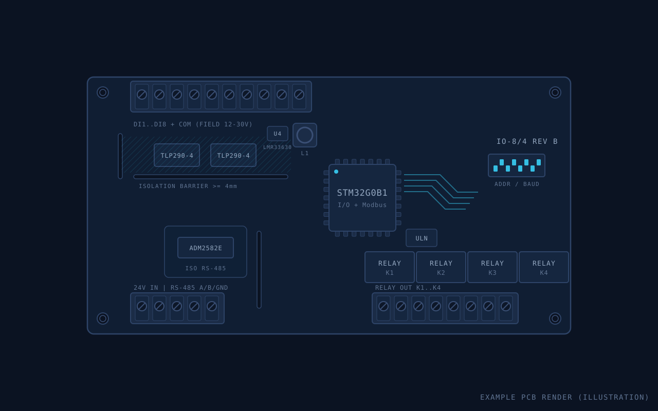
DIN-rail I/O controller with eight isolated digital inputs, four relay outputs and a Modbus RTU slave interface, designed for retrofit into existing 24 V control cabinets. (Fictional example content.)
Product requirements
- Eight isolated 24 V digital inputs tolerant of 12–30 V field wiring; four relay outputs rated 5 A resistive.
- Modbus RTU slave on RS-485, 9.6–115.2 kbaud, response inside 10 ms at any supported rate.
- 18–36 V DC supply input with reverse-polarity protection and EFT/surge immunity per the relevant IEC 61000-4 levels.
- Configuration (address, baud, watchdog behaviour) via DIP switches plus holding registers, retained across power cycles.
- Fail-safe: relays drop to a defined state if bus communication stops for a configurable timeout.
System architecture
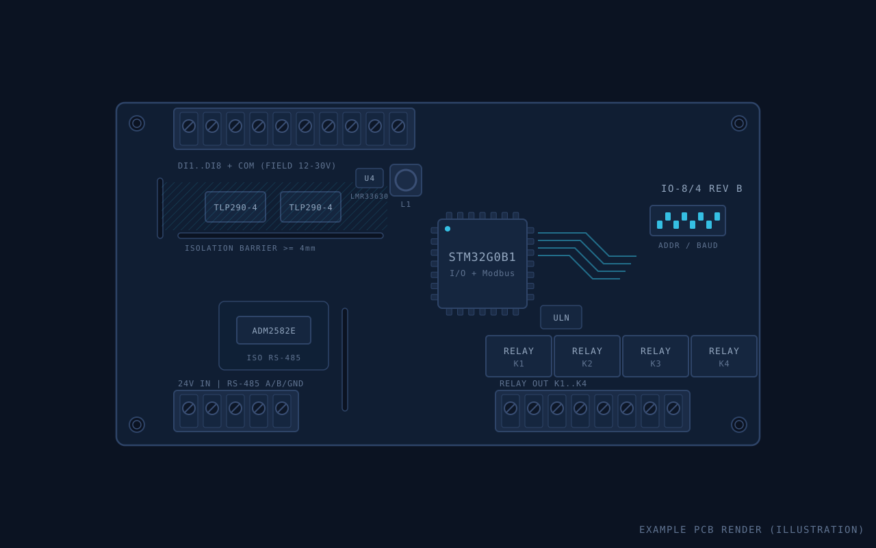
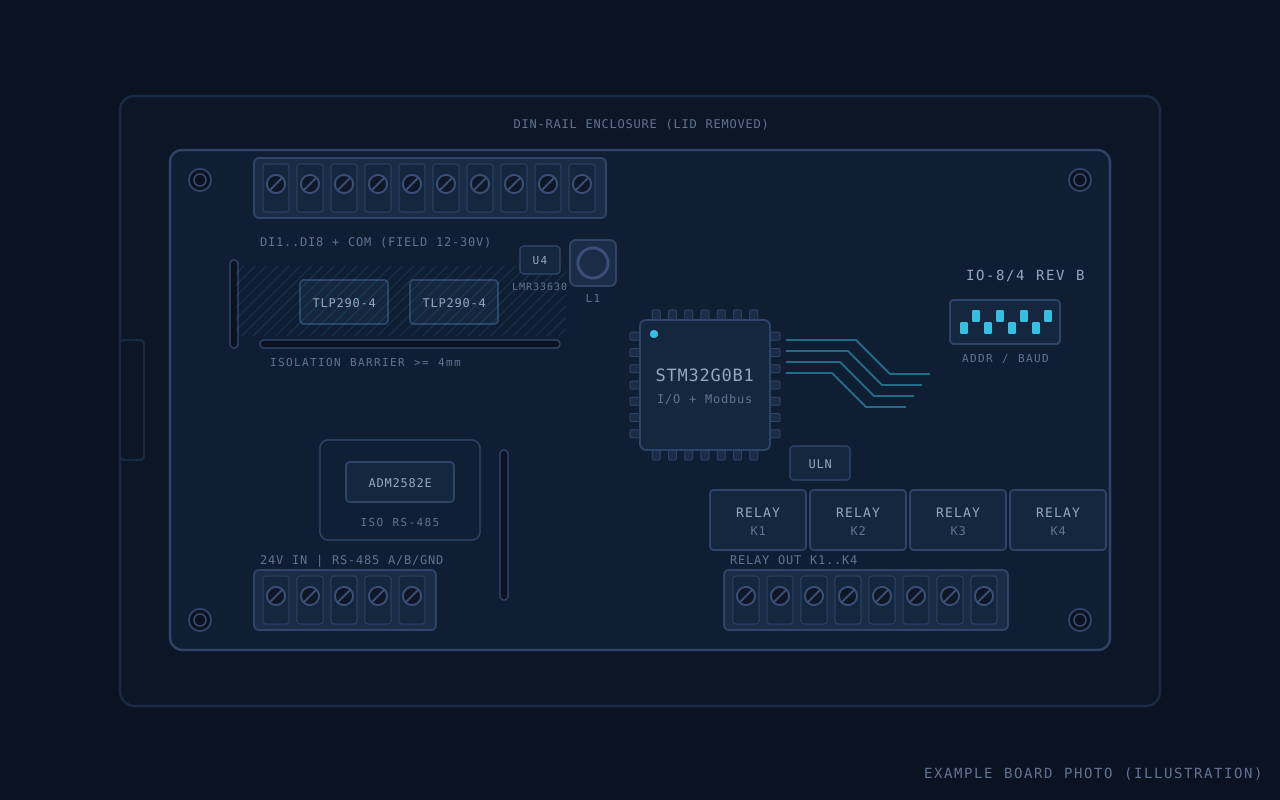
An STM32G0B1 runs the register map, I/O scan and Modbus stack. Field inputs pass through per-channel conditioning into two quad optocouplers; relays are driven by a ULN2003A with per-coil flyback handling. The RS-485 transceiver is a galvanically isolated ADM2582E with its integrated isolated supply. A wide-input buck converter generates 5 V for relays and logic, followed by a 3.3 V LDO for the MCU. The PCB is partitioned into field, bus and logic zones with isolation gaps sized to the target creepage class.
Hardware design
- Per-input RC filtering and current limiting ahead of the optocouplers, with thresholds set for reliable 12 V operation and 30 V continuous tolerance.
- Relay coil supply switched separately so a fail-safe drop is guaranteed by hardware, not only by firmware.
- TVS, common-mode choke and fuse network at the supply input for the surge/EFT levels; RS-485 pair protected by a dedicated transient suppressor.
- Isolated RS-485 with selectable termination and fail-safe biasing via DIP switch.
- All connectors as pluggable terminal blocks, arranged so field and bus wiring exit opposite ends of the enclosure.
Firmware features
- Bare-metal Modbus RTU slave (function codes 01–06, 15, 16) with a documented register map.
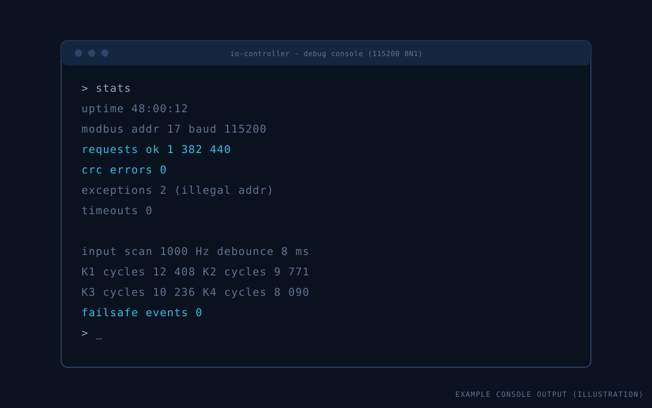
- 1 kHz input scan with per-channel debounce configurable via holding registers.
- Communication watchdog driving the fail-safe relay state, with cause logged in an event register.
- Configuration stored in EEPROM emulation with wear-levelled pages and CRC-protected records.
- Cycle counters per relay and a diagnostics register block for fleet maintenance planning.
Testing process
- Automated functional test cycling every input and relay through a bench jig with pass/fail logging.
- 48-hour Modbus soak at 115.2 kbaud with induced noise, tracking CRC-error and timeout counters.
- Pre-compliance EFT/burst testing on supply and bus ports at the target severity levels.
- Thermal survey at 36 V supply with all relays energized in a closed enclosure.
- Fail-safe timing verification: measured delay from bus silence to defined relay state across the configurable range.
Technical challenges
- EFT bursts on the field wiring caused occasional MCU resets through ground coupling on the first revision.
- Relay switching produced disturbances on the RS-485 pair that corrupted frames at the highest baud rate.
- The 10 ms response requirement conflicted with EEPROM-emulation write stalls when configuration writes landed mid-poll.
Solutions implemented
- Re-partitioned the ground scheme with a single controlled field-to-logic reference point and moved the input filters right to the connector edge; resets no longer reproducible at the target test level.
- Added snubbing at the relay contacts, rerouted the bus pair away from the relay bank and tightened the transceiver's fail-safe biasing; error counters clean at 115.2 kbaud over the full soak.
- Deferred EEPROM commits to a low-priority idle slot with a dirty-flag scheme, keeping worst-case Modbus response inside the requirement.
Final outcome
Revision B passed the full functional, soak and pre-compliance test plan. Units from the pilot assembly run were handed over with the manufacturing package and the register-map documentation. (Fictional example outcome.)
Deliverables
- Altium source files and generated manufacturing package (Gerbers, drill, pick-and-place)
- BOM with approved alternates
- Firmware source with unit tests, register-map and configuration documentation
- Functional-test jig firmware and test procedure
- Pre-compliance test report
Gallery
Building something similar?
I take on firmware, hardware and PCB design projects at any stage of development.
Discuss Your Project