Sample Project: CAN Bus Vehicle Accessory Module
12 V accessory controller for special-purpose vehicles: four protected high-side outputs driven from CAN commands, with sleep/wake on bus activity and load diagnostics. (Fictional example content.)
Product requirements
- Operate from a nominal 12 V vehicle supply, surviving load dump, reverse polarity and the relevant ISO 7637-2 pulses.
- Four high-side outputs, 3 A continuous each, with open-load and overcurrent detection reported over CAN.
- CAN 2.0B at 500 kbit/s using a defined application message set; CAN-FD capable hardware for future use.
- Sleep below 100 µA with wake on CAN activity or ignition sense.
- Operating range −40 to +85 °C, parts selected accordingly.
System architecture
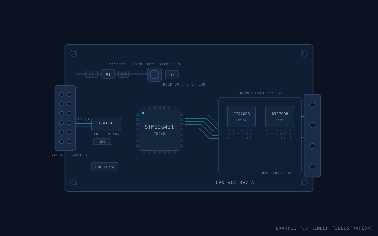
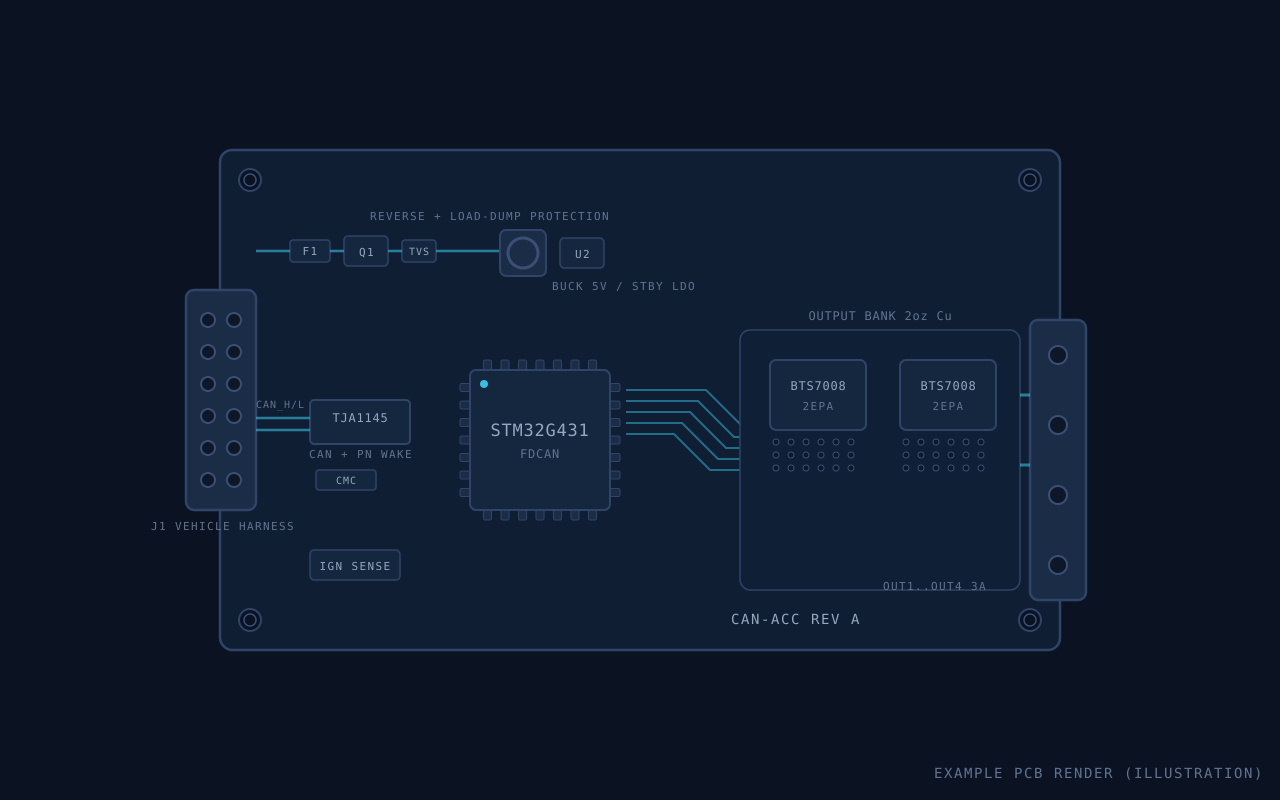
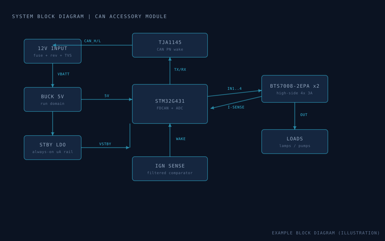
An STM32G431 with its FDCAN peripheral pairs with a TJA1145 transceiver whose partial-networking wake keeps the module asleep until addressed. Outputs use BTS7008-2EPA dual high-side switches with per-channel current sense fed to the MCU ADC. The power input chain is fuse, reverse-blocking MOSFET and load-dump-rated TVS into a buck regulator, with a separate always-on micro-power rail for the standby domain. Ignition sense enters through a filtered, clamped comparator input.
Hardware design
- Input protection network validated against the selected ISO 7637-2 pulse set; load-dump energy shared between the TVS and the regulator's input rating.
- High-side switches placed on a widened-copper bank with thermal vias, keeping junction temperatures modelled inside limits at 3 A per channel at +85 °C ambient.
- Current-sense scaling chosen so both open-load (light load) and overcurrent thresholds resolve within the ADC range.
- CAN pair routed as a 120 Ω differential pair with a common-mode choke and ESD clamp at the connector.
- Automotive-qualified (AEC-Q) parts used for all silicon in the supply and I/O paths.
Firmware features
- FreeRTOS application: CAN task, 1 kHz output-control/diagnostics task and a background self-test task.
- Application message handling with command timeout: outputs revert to a safe state if command frames stop.
- Per-channel soft-start PWM ramp to tame inrush into lamp and pump loads.
- Fault manager latching overcurrent trips with retry policy and CAN-reported diagnostic codes.
- Sleep manager driving the TJA1145 into partial-networking standby; wake source recorded and reported.
Testing process
- Bench validation of every output channel against resistive, lamp and inductive loads across the supply range.
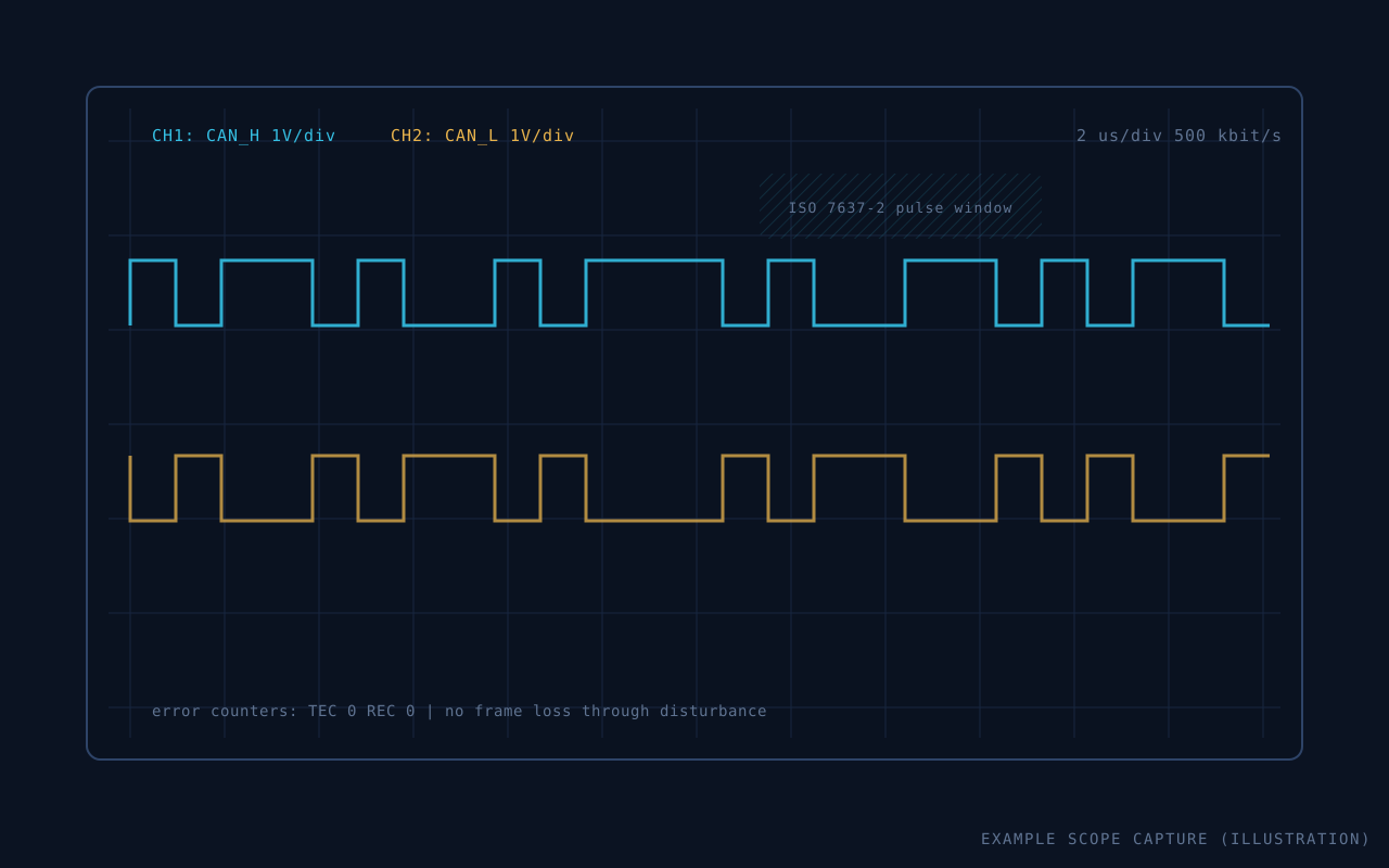
- Supply-transient testing with replayed ISO 7637-2 pulses while monitoring CAN traffic for errors and resets.
- Sleep-current measurement across temperature corners in a small environmental chamber.
- Wake-latency measurement from CAN frame to first valid status response.
- Thermal imaging of the output bank at sustained 3 A per channel.
Technical challenges
- Sleep current measured well above target on revision A, traced to the current-sense dividers remaining powered in standby.
- Inductive-load turn-off produced negative transients that occasionally reset a high-side channel's diagnostics.
- A ground-offset condition between vehicle harness points corrupted low-load open-circuit detection thresholds.
Solutions implemented
- Gated the sense dividers behind a small load switch controlled by the standby domain; sleep current landed under the 100 µA target with margin.
- Added per-channel freewheeling clamping suited to the specified inductive loads and masked diagnostics during the defined demagnetization window.
- Re-referenced open-load detection to a ratiometric threshold using the local supply measurement instead of a fixed voltage.
Final outcome
The prototype batch completed the bench validation plan and was handed over for vehicle-level trials, together with a findings list feeding the planned production redesign. (Fictional example outcome.)
Deliverables
- KiCad source files and manufacturing outputs for the prototype revision
- Firmware source with the CAN application message documentation
- Bench validation report and thermal survey
- Findings and recommendations list for the production redesign
Gallery
Building something similar?
I take on firmware, hardware and PCB design projects at any stage of development.
Discuss Your Project